
Solder Paste Stencil in PCB Assembly
PCBA circuit boards rely on a complex network of lines to integrate various hardware devices into one integrated unit. The lines, also known as traces, carry electrical signals from components to the next layer of the board and back again. The function of a solder paste stencil is to ensure that the correct amount of solder is placed on each pad. This is critical for accurate and reliable operation of the circuit board. Stencils are manufactured using a variety of fabrication techniques including laser cutting and chemical etching.
Stainless steel and nickel are commonly used materials for stencils due to their durability and resistance to chemicals. The thickness of a stencil is critical and will vary depending on the specific application requirements – fine pitch devices require thinner stencils while large component parts require thicker ones. Rounding the edges of stencil apertures improves paste transfer and reduces bridging between pads.
Once a stencil has been designed it must be carefully inspected to ensure that each pad is appropriately covered by paste. This is especially important for ICs and other small components that may have multiple pads. If a pad is left uncovered it can cause defects during reflow and result in unreliable connections.
The thickness of the stencil is a key parameter that plays a significant role in achieving optimal paste deposition and ensuring that the proper amount of solder is applied to each pad. The optimum thickness will vary depending on the specific application and manufacturing process.
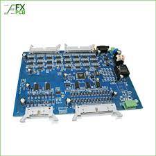
The Role of a Solder Paste Stencil in PCB Assembly
In order to ensure that the stencil is able to perform optimally, it must be regularly cleaned and maintained. This includes cleaning the apertures and removing accumulated solder, flux residues and other contaminants. In addition, the stencil should be stored in a clean environment and handled carefully to prevent bending or damage that could compromise its performance.
Once the stencil has been cleaned and maintained it can be used to apply the solder paste to the surface mount components on the circuit board. The stencil must be carefully aligned with the pcba circuit board to ensure that each hole is adequately populated with paste. Once the alignment is complete a metal squeegee blade can be used to spread the paste over the pads of the circuit board.
In addition to the size and shape of the stencil apertures, the type of paste being used will have an impact on the performance and reliability of the assembly. Different paste types have different viscosity and will require a different paste thickness and aperture opening ratio.
Stencil maintenance involves routine cleaning, inspection, and rework or replacement as needed to uphold optimum performance and reliable paste deposition. The process of rework or replacement involves the use of an appropriate solvent or chemical to remove any material that has built up in the stencil apertures. This process is essential to preventing blockages in the apertures that can hinder paste flow or lead to uneven deposits. Regular cleaning and maintenance will also extend the lifespan of a stencil.


